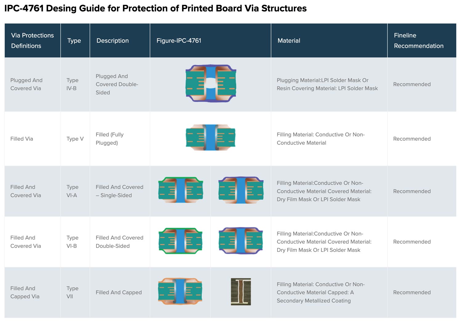
| Via Protections Definitions | Type | Description | Figure-IPC-4761 | Material | Fineline Recommendation | |
|---|---|---|---|---|---|---|
| Plugged and Covered Via | Type IV-b | Plugged and Covered Double-sided |  |
Plugging material:LPI solder mask or Resin Cover material: LPI solder mask |
Recommended | |
| Filled Via | Type V | Filled (fully plugged) |  |
Filling material: Conductive or non-conductive material | Recommended | |
| Filled and Covered Via | Type VI-a | Filled and Covered – Single-Sided |  |
 |
Filling material:Conductive or non-conductive material Cover material: Dry film mask or LPI solder mask |
Recommended |
| Filled and Covered Via | Type VI-b | Filled and Covered Double-sided |  |
 |
Filling material:Conductive or non-conductive material Cover material: Dry film mask or LPI solder mask |
Recommended |
| Filled and Capped Via | Type VII | Filled and Capped |  |
 |
Filling material: Conductive or non-conductive material Capped: a secondary metallized coating |
Recommended |
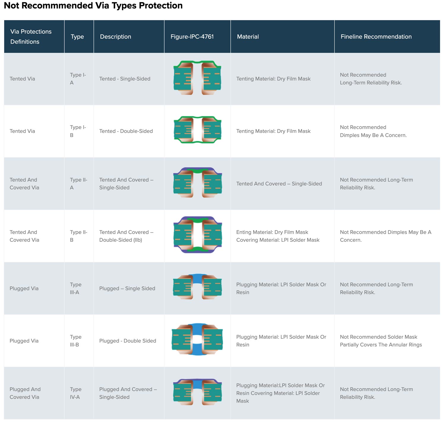
| Via Protections Definitions | Type | Description | Figure-IPC-4761 | Material | Fineline Recommendation | |
|---|---|---|---|---|---|---|
| Tented Via | Type I-a | Tented - Single-Sided |  |
Tenting material: Dry film mask | Not Recommended Long-term reliability risk. |
|
| Tented Via | Type I-b | Tented - Double-Sided |  |
Tenting material: Dry film mask | Not Recommended Dimples may be a concern. |
|
| Tented and Covered Via | Type II-a | Tented and Covered – Single-Sided |  |
Tented and Covered – Single-Sided | Not Recommended Long-term reliability risk. | |
| Tented and Covered Via | Type II-b | Tented and Covered – Double-Sided (IIb) |  |
Tenting material: Dry film mask Covering material: LPI Solder mask |
Not Recommended Dimples may be a concern. | |
| Plugged Via | Type III-a | Plugged – Single Sided |  |
Plugging material: LPI solder mask or Resin | Not Recommended Long-term reliability risk. | |
| Plugged Via | Type III-b | Plugged - Double Sided |  |
Plugging material: LPI solder mask or Resin | Not Recommended Solder mask partially covers the annular rings | |
| Plugged and Covered Via | Type IV-a | Plugged and Covered – Single-Sided |  |
Plugging material:LPI solder mask or Resin Cover material: LPI solder mask |
Not Recommended Long-term reliability risk. | |