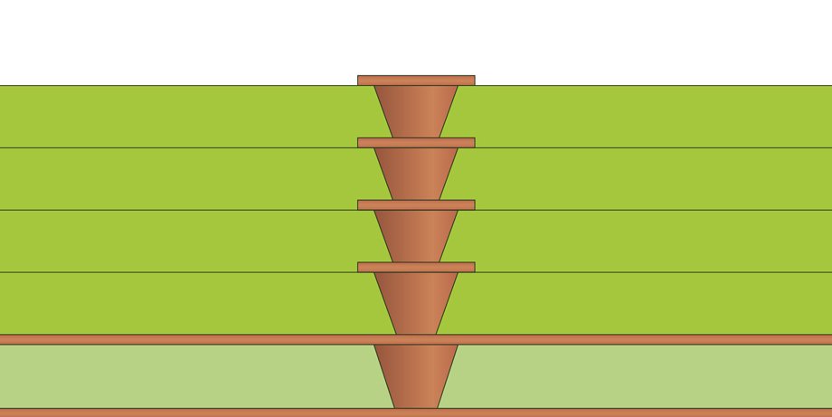
From 1+N+1 to X+N+X stack-ups, “all layer” technology and in a wide range of technological variants.
An HDI PCB is a PCB which has a far higher wiring density than a conventional through hole PCB. Per IPC-6012 (1.4.1) this is defined as a design which has an average number of electrical connections/cm² of 20 or more, on both sides of the PCB.
An HDI PCB uses finer features than a conventional PCB, enabling tighter packaging densities and lower layer count and/or reduced size. All HDI PCBs should follow IPC2226 – Sectional Design Standard for High Density Interconnect (HDI) Printed Boards. IPC2226 separates HDI into types I to type VI depending on usage and complexity.
Typical applications are smartphones, where space is at a premium, and aerospace where smaller size and/or reduced weight are key drivers.