Every customer application is different, and the design determines the execution. Your design and the type of technology are usually determined by you before you talk to us.
This also means that about 80% of the cost of the PCB is determined in advance.
Over-designed PCBs cost more and limit production capabilities. If you talk to us, at an early stage, we can offer cost-effective design and manufacturing options to deliver the best technology solution, along with a commercial advantage.
We strive to reduce complexity and ensure that the design is an appropriate use of the technology.
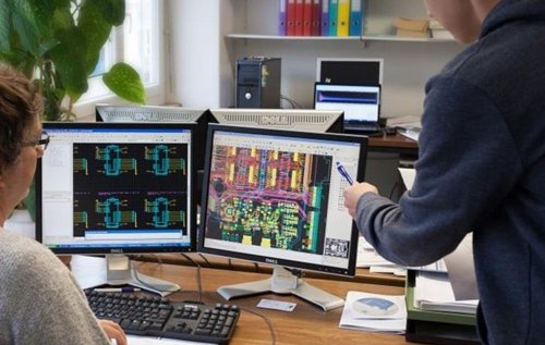
Sometimes customers need more support. It might be a broader design service, or that they are unfamiliar with one of the PCB technologies, or even that their internal team are overloaded. For these customers we can often provide design advice and even complete design including R&D and layout.
Contact us at any stage and we will advise and support you in achieving your design goals.
Design For Manufacture
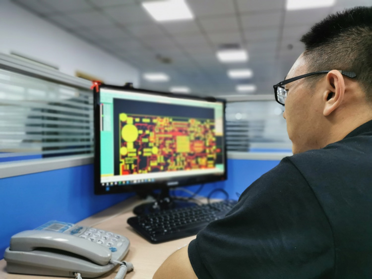
Design for Manufacture (DFM) realises maximum benefits when both you and the supplier are aware of the requirements from the outset. From a comprehensive design brief and initial discussions prior to layout, material set(s) can be reviewed and agreed, which become the foundation onto which the design is ultimately built.
Technology requirements such as HDI and rigid flex can also be reviewed, together with compatibility with other special features e.g. resin filling of vias. Even recommendations on minimum feature sizes such as track/gap, laser drill via sizes and pad diameters can all be defined and agreed in order the transition into prototype and volume manufacture is virtually seamless.
On existing designs the same process can be followed, though this is not DFM in its true sense – but more reverse engineering or design optimisation. We can review material requirements and recommend suitable lower cost alternatives, still meeting the same specification requirements.
Likewise, we will consider optimisation of feature sizes, with the aim of increasing yields and reducing cost. Panelisation can also be reviewed to give best compromise between PCB and PCBA and even surface finish where, for example, a simple part with no fine pitch components has fabrication notes calling for ENIG, alternative lower cost finishes can be proposed.
We always aim to offer options to reduce costs, when we can, to provide you with value engineering.
Fineline is a reliable partner with extensive know-how and capabilities in the industry.
Their commitment towards quality and customer service
helped us in always achieving all our objectives