Given the vast amount of information and details, consolidating all the DRC/DFM rules in a one-pager would not only be an impractical undertaking but also an infeasible one. To help guide our existing and potential clients through the maze of PCBs, in this document we focus on the most important ground rules.

All successful projects, in any sector, start with a strong team and share a similar set of processes and procedures. PCBs are no different. Creating a solid layout, taking into account all relevant considerations including the smallest details to support a reliable, fully automated assembly, with mass production in mind, is what generates state-of-the-art PCBs. In some cases, the components and the stages of this planning can contradict one another, but at Fineline we pride ourselves for being problem solvers.
1. THE SCHEMATICS LEVEL
It starts at the schematics level – the engineer putting together the schematics has to be very clear, to the point, and available to the layout engineer for questions. In schematics:
- Keep the “in” and “out” directions consistent. If the direction is kept when placing the parts, then when working on the common or return path as well, it will make the design work smoothly. Ignoring the directions would cause issues.
- Group parts that need to be together close to each other. If using hierarchical designs, try not to have a large part split between pages if possible (mainly parts with large number of pins). If you must do so, gather on each page the other parts accordingly, especially the battery capacitors, filter capacitors, etc. Having many filtering caps on one page will make it extremely difficult to get them placed correctly. If you have different capacitance values but the same footprint, it is a placement challenge. Communicate these to the layout engineer.
- Add text. It won’t show on the netlist, and it is not a constraint transferred by the capture/layout tools, but if it is important enough – it worth writing it down (and later verify during design review).
- When you generate a schematic capture, make it so the layout designer who will work on it will understand its language, and will not need you to constantly be there during the layout, not even for placement.


2. FOOTPRINTS
- Try to use the most reliable packages available. If you can put a 0402, don’t use a 0201. If you can choose a BGA, don’t use a QFN. The reliability and robustness of a design are derived by it.
- Make sure that on the schematics level, the package you chose for each part is clear, even when there is more than one option.
- Maintain an approved library based on ordering PN. It might mean the same JEDEC footprint resides in the library a dozen times, but then you will also know you got the right one on the screen. Using generic footprints may cause geometry issues or worse – using a completely wrong one. We all know that disk space nowadays is pretty much cost-free.
- Use state-of-the-art tools to build a footprint. IPC-7351 is a great standard to comply with.
3. MECHANICAL CONTROL DRAWINGS
- Have TWO mechanical control drawings. This is crucial. There are many processes to build a board; however, the manufacturing facility that makes the bare board needs to know the critical dimension for PCB making, and not the layout. For instance, if you crowd one drawing with all the instructions for the layout (hole locations, component height restrictions, where to put labels, etc.) it will be difficult for the PCB manufacturer to make sure, in his quality assurance and programming, that all the critical dimensions for YOUR PCB have been followed and verified. It’s always better to separate the essential information for PCB making from the ones for layout.
4. BILL OF MATERIALS
- Many times, the density of a design forces a layout designer to choose between two “evils.” A smart schematics designer will make sure parts that are added for provisioning, such as a pull-up or a pull-down and non-critical path parts, will be known to be so. Add a list of parts that will appear on the layout but are not going to be having any actual parts on them.
5. CONSULT WITH YOUR SUPPLY CHAIN PARTNERS
- When starting a design, think of the partners you have and what they would like to get from you. Ask them to participate in designing a stack-up as early as possible in the design phase. Get from them material availability for your design, to prevent long lead time for materials when your operations will place an order. Ask your partners to verify and calculate for you impedances for your critical paths, based on materials they use. Check with them several options for what materials to use. It might be that expensive materials aren’t needed. Can they design a hybrid? Can board thickness be met with all the geometry constrains for impedances? The sooner you have the information, the cleaner your layout will be. It will help you to keep symmetric stack-ups too. For example, can the tolerance you ask be met?
6. GET REQUIREMENTS FROM YOUR EMS PARTNER
- Volg hun regels, zodat ze u beter van dienst kunnen zijn en minder problemen hebben tijdens de assemblage. Niet alleen de kosten zullen dalen tijdens de assemblage, maar uw product zal ook betrouwbaarder zijn en voldoen aan de vereiste normen. Plaats de onderdelen op de printplaat als u hun aanbevelingen opvolgt (houd rekening met een binnenplaats rond onderdelen voor pick-and-place, houd onderdelen uit elkaar voor verschillende processen zoals SMT, Press-fit, en waive-soldeer, etc.).
7. USE THICK TRACES WHEN YOU CAN
- While suppliers may tell you that they can go with 3 mil traces and 3 mils spacing, note that the cost will be higher, because the yields are lower. Go with 5-6 mils if you can, and 5-6 mil spacing. Narrow down if you have no other choice.
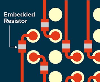
8. COPPER
- In your eyes, copper is free. Keep as much copper in your design, and avoid the need to etch large areas of copper. Alternatively, allow suppliers to add thieving bars to balance the layout, if you can’t do it yourself. Unbalanced copper percentage per layer is a recipe for shorts between adjacent layers with small dielectric distance.
9. PANEL DESIGN
- A good designer would also add a panel design for proper assembly, while an even better designer would add the necessary means for proper depanelizing. The perfect designer will do it both and also consult with his PCB supplier regarding getting as much raw material used to reduce cost, when designing the step and repeat. Check the panel size your supplier uses!
10. REMEMBER
- Your supply chain partners are on your team. Work with them to get better results.
There are many more consideration to take into account, and we, at Fineline, are connoisseurs of this process. We have the team to support you. Contact our local office with any questions you might have and they will refer you to the appropriate, knowledgeable expert.