Why Do PCB Jobs Go On Hold?
There is an extensive amount of precise data needed to build a Printed Circuit Board. As the layer count and complexity increase, so does the amount of correct information needed by the PCB fabricator to properly manufacture the job. If any part of the data is missing, the CAM operator will hand the file back to sales to sort out the problems. Your much-needed PCB job goes on hold.
DON'T GUESS IN PRINTED CIRCUIT BOARD MANUFACTURING
The one rule that all PCB manufacturing facilities hold strong and dear to their heart is, we don’t guess. If you break the rule, it is guaranteed to bite you hard. To ensure no one is guessing, every question has to be answered. If there is a tolerance missing on a set of holes, the job will go on temporary hold until the CAM person can get a suitable answer. If there is an electrical short between ground power layers due to a misplaced via, the job goes back to sales to sort out. When a job is on hold for a serious problem it can cause days of delay. If there are one or two small issues, usually the CAM operator or sales will call and sort it out. A trace or two can be moved to prevent a short, or a pad size increased to correct a problem with too small an annular ring. However, the CAM operator has to get their quota of x number of jobs out each day to keep the manufacturing facility fully loaded. The CAM operators do not have a lot of time to fix a mirage of problems in the data. In that scenario, the CAM operator hands the file back to sales for them to reject the data and request the customer fix the problems then resubmit it through the whole process of quotation and the design rule check in PCB and set up.
COMMON MISTAKES RESULTING IN JOB ON HOLD
Some of the more common mistakes that result in jobs going on hold are:
- Missing data, a drill file
- Solder mask or nomenclature white marking file not in the CAD package. (common)
- Missing or wrong information on drawing of outside dimensions
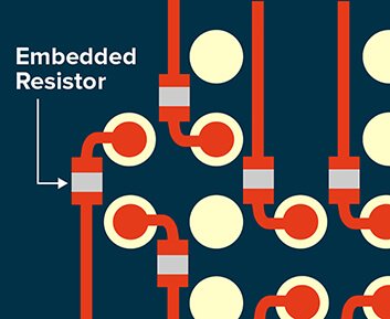
- Missing specifications of laminate, in hole plating and surface finishes (very common)
- Shorts or space violations in trace spacing (difficult for the CAM engineer to fix easily)
- Hole size in relationship to pad size too small, violating clearance spacing between pads
- Spacing violations of clearance of solder mask around pads (common)
- White identification nomenclature marking across pads (common)
- Improper sequence of drilled holes in a buried via multilayer
- Hole sizes too small or too large, in relation to pad size and annular ring requirements (common)
- Through via holes short out ground planes to power planes (common)
- Specifying a square inside corner in final routing (router bits are round)
- As PCB requirements get more complicated, more missing information and technical items start to become even more important and are quite often not specified. A very common error is where a particular impedance is specified, but it cannot be met due to thickness of material or Dk of the specified material.
These examples and many more, result in the job going on hold and multiple calls/emails can be required to answer the questions, causing additional delay.
PCB JOBS AT FINELINE
Een bepaalde klant leek altijd in de 'afgewezen in de wacht' bak bij de verkoopbalie te zitten. Na een stressvolle eerste ontmoeting vroegen ze waarom hun printplaten altijd in de wacht stonden bij ons, terwijl een andere PCB-fabrikant ze gewoon bouwde. Ons engineering team liep met hen door wat ze misten op het tekeningenpakket. Een punt dat ze naar voren brachten was dat de printplaten die ze van verschillende fabrikanten kochten op verschillende manieren werkten. Er werd op gewezen dat, omdat hun specificatieblad voor printplaten zo ontbrak, de andere printplaatfabrikanten hen verschillende laminaten gaven die zij in voorraad hadden. Er werden verschillende platingdiktes geproduceerd omdat dit niet was gespecificeerd en er werden verschillende soldeermaskers gebruikt. Onze ingenieurs legden zorgvuldig uit waarom dit kleine wijzigingen zijn die een fabrikant van printplaten kan aanbrengen als ze niet gespecificeerd zijn. Tijdens de lange vergadering werden de kopers en ontwerpers erop gewezen dat een eenvoudige verandering in laminaat, soldeermasker en platingdikte de impedantie aanzienlijk zou veranderen. Zij kwamen overeen om op de fabricagetekening een bepaald laminaat te specificeren dat een stabiele leverancier had en bekend stond om zijn kwaliteitsprodukt. De CAD-manager liet hen zien hoe een verandering in de gespecificeerde laagdikte hun opbrengst en toekomstige betrouwbaarheid zou beïnvloeden, en als zij een minimale laagdikte van 1,2 mils koper in het gat zouden specificeren, zou dat hun opbrengst uit golfsolderen aanzienlijk verbeteren, en de thermische levensduur verlengen, hopelijk een van hun grootste problemen oplossend. Naarmate de vergadering vorderde, vroegen wij om meer dan twintig aanvullingen en veranderingen in de technische specificaties van de bouwplaat en om meer technische gegevens aan hun technische tekeningen toe te voegen om een strakkere set specificaties te garanderen.
De fabrieksdirecteur nam hen mee voor een rondleiding door de fabriek voor de productie van printplaten en liet hen zien waarom wij niet gissen. Eerst kregen ze de opslagruimte voor laminaten te zien, waar letterlijk honderden verschillende soorten laminaten lagen, elk met twintig verschillende diktes en kopergewichten. Tijdens de rondleiding door de rest van de fabriek zagen de ingenieurs en inkopers zo veel verschillende manieren om hetzelfde product te maken. Ze begrepen volledig waarom er zo veel strikte specificaties nodig zijn wanneer een meer kritische printplaat vereist is. Ze apprecieerden alle informatie die nodig was om hun Printed Circuit Board bestelling uit de gevreesde wachtmand te houden.