Delivering Technologically Advanced Processes
Fineline specialises in the production of PCBs, delivering technologically advanced processes, and providing the market with an extensive catalogue of products suitable for any electronic application.
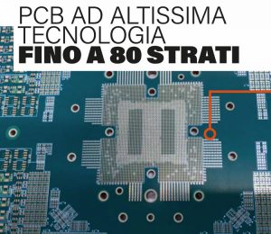
HIGH-TECH PCB UP TO 80 LAYERS
Fineline deals in PCBs of all types: from the simplest single-sided and double-sided to the more complex, such as HDI, rigid-flex and PCBs for ATE boards – all with guaranteed quality and reliability, at a competitive price. We can also provide PCBs for testing in semiconductor manufacturing to support any platform or tester.

Our technical team’s skills allow us to supply PCBs with over 80 layers and aspect ratios of up to 50:1, so that customers can test devices with ever more advanced technologies and ever reducing features. Being a part of Shenzhen Fastprint Circuit Tech Co., Ltd enables us to support these advanced technologies. We also work directly with Harbor Electronics who have facilities both in California’s Silicon Valley and Harbor China located in Fastprint Technology Park in Guangzhou.
Types of printed circuit boards for semiconductors. There are several types of printed circuit boards required for semiconductor testing which Fineline can supply:
PROBE CARD:
- Used to connect the various platforms of testers to the device pads present on the wafer. The probe card is adaptable to the main testing platforms which enables verification of the quality of wafers, the packaging of integrated circuits and the quality of the chips, thereby avoiding packaging costs due to defective products.
INTERPOSER:
- The interposer, or space transformer, is a PCB that allows you to reduce the pitches on the pads and tracks on the probe card down to dimensions approaching those of the wafer pads.
LOAD BOARD:
- A load board is used for final tests in the same manner a probe card is used to connect the various tester platforms to the integrated circuits after packaging. This ensures verification and full functionality of the working component is validated.
BIB (Burn-In-Board):
- The Burn-In-Board is used to verify reliability and to perform ageing tests (under specific operating conditions and over a specific period of time) on integrated circuits that have completed their packaging tests.Within the semiconductor manufacturing process, Fineline’s PCBs are used in the test phase after wafer production, until the device is validated in its final application.
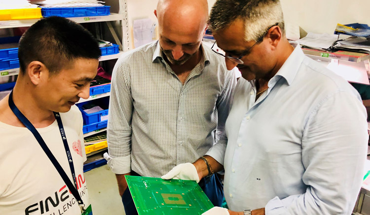
Fineline technicians together with the technical staff at the production plant working on an ATE PCB project
The plant for ATE Board is called Harbor Electronics
Harbor Electronics was founded in the 1980s and started producing highly specialised printed circuit boards for the ATE industry in 1995. Based in Santa Clara, California, Harbor Electronics is renowned worldwide as a specialist in advanced printed circuit boards for the semiconductor test market. In 2015, Harbor joined forces with Shenzhen Fastprint Circuit Tech, thereby creating the world’s largest supplier of PCBs for this market segment. Our customers are the largest companies in the semiconductor industry. With two plants, one in China and one in the United States, both with advanced production capabilities, our customers can keep up to date with the ever-changing technology and innovation in semiconductor production.
Luca Giovelli is the Managing Director of Fineline Italy S.r.l.