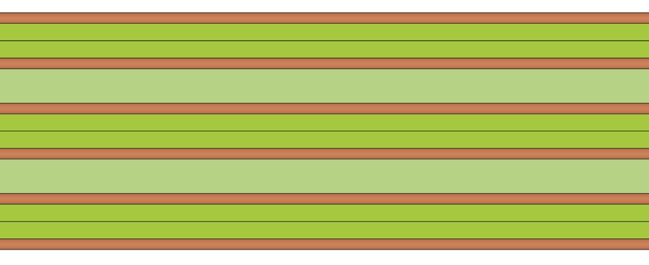
Multilayer PCB Without Solder Resist

Multilayer PCB With Solder Resist
A multilayer PCB will, by definition, have 3 or more conductive copper layers, each separated from the others using either fully cured core material, or partially cured prepreg material. A multilayer PCB is more complex and dense than either single sided or double sided PCBs and can be used for higher technology applications. Using alternate core and prepreg materials, the required multilayer stack is created and copper foils used to form what will become the top and bottom layers of the PCB. The application of heat and pressure in the bonding press fully cures the prepreg material to create the finished multilayer. PTHs take connections from layer to layer in the same manner as a double sided PCB.
Advantages of a multilayer PCB over both single sided and double sided include:
This is one example. Every application is different so please contact our experts to discuss your requirements, in full.
From engineering advice to selecting the right manufacturing partner for
you – our experience and expertise gives you the right solution.
Get in touch and let’s start working together.