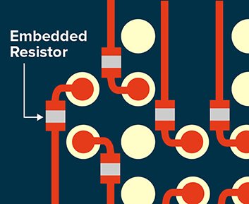
Embedded Resistors in Printed Circuits: Fineline Global Commitment to Innovation and Advancing Technology
By: Maysa Salameh, Chief Technology Officer, Fineline Global
Explore more
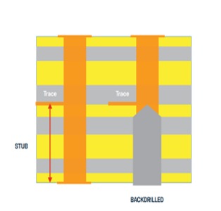
Multilayers: Design Rules
Explore more
Embedded Resistors / Capacitors Technology
All about embedded resistors and capacitors technology
Explore more
Optimised PCB Design – Design Rules In Your Layout System
Explore more